CHAPTER NO: 1
INTRODUCTION TO PCI BUS
1.1 PCI Overview
1.2 PCI Bus Protocol
1.3 PCI Signal Descriptions
System Pins
Address and Data Pins
Interface Control Pins
Arbitration Pins (Initiator Only)
Error Reporting Pins
Interrupt Pins
Cache Support Pins (Optional)
64-Bit Bus Extension Pins (Optional)
1.4 PCI Bus Timing Diagrams
Read Transaction
Write Transaction
1.5 PCI Connector Pinout
1.1 PCI Overview
The PCI Local Bus is a high performance bus for interconnecting chips, expansion boards, and processor/memory subsystems. It originated at Intel in the early 1990s as a standard method of interconnecting chips on a board. It was later adopted as an industry standard administered by the PCI Special Interest Group, or "PCI SIG". Under the PCI SIG the definition of PCI was extended to define a standard expansion bus interface connector for add-in boards.
PCI was first adopted for use in personal computers in about 1994 with Intel's introduction of the "Saturn" chipset and "Alfredo" motherboard for the 486 processor. With introduction of chipsets and motherboards for the Intel Pentium processor, PCI largely replaced earlier bus architectures such as EISA, VL, and Micro Channel. The ISA bus has initially continued to co-exist with PCI for support of "legacy" add-in boards that don't require the high performance of the PCI bus. But as legacy boards are redesigned, PCI is expected to completely replace ISA as well.
1.2 PCI Bus Protocol
PCI is a synchronous bus architecture with all data transfers being performed relative to a system clock (CLK). The initial PCI specification permitted a maximum clock rate of 33 MHz allowing one bus transfer to be performed every 30 nanoseconds. Later, Revision 2.1 of the PCI specification extended the bus definition to support operation at 66 MHz, but the vast majority of today's personal computers continue to implement a PCI bus that runs at a maximum speed of 33 MHz.
PCI implements a 32-bit multiplexed Address and Data bus (AD[31:0]). It architects a means of supporting a 64-bit data bus through a longer connector slot, but most of today's personal computers support only 32-bit data transfers through the base 32-bit PCI connector. At 33 MHz, a 32-bit slot supports a maximum data transfer rate of 132 MBytes/sec, and a 64-bit slot supports 264 Mbytes/sec. Although it is not widely implemented, PCI supports 64-bit addressing. Unlike the 64-bit data bus option, which requires a longer connector with an additional 32-bits of data signals, 64-bit addressing can be supported through the base 32-bit connector. Dual Address Cycles are issued in which the low order 32-bits of the address are driven onto the multiplexed Address and Data bus allows a reduced pin count on the PCI connector that enables lower cost and smaller package size for PCI components. Typical 32-bit PCI add-in boards use only about 50 signals pins on the PCI connector of which 32 are the multiplexed Address and Data bus. PCI bus cycles are initiated by driving an address onto the AD[31:0] signals during the first clock edge called the address phase. The address phase is signaled by the activation of the FRAME# signal. The next clock edge begins the first of one or more data phases in which data is transferred over the AD[31:0] signals.
In PCI terminology, data is transferred between an initiator, which is the bus master, and a target, which is the bus slave. The initiator drives the C/BE[3:0]# signals during the address phase to signal the type of transfer (memory read, memory write, I/O read, I/O write, etc.). During data phases the C/BE[3:0]# signals serve as byte enable to indicate which data bytes are valid. Both the initiator and target may insert wait states into the data transfer by deasserting the IRDY# and TRDY# signals. Valid data transfers occur on each clock edge in which both IRDY# and TRDY# are asserted.
A PCI bus transfer consists of one address phase and any number of data phases. I/O operations that access registers within PCI targets typically have only a single data phase. Memory transfers that move blocks of data consist of multiple data phases that read or write multiple consecutive memory locations. Both the initiator and target may terminate a bus transfer sequence at any time. The initiator signals completion of the bus transfer by deasserting the FRAME# signal during the last data phase. A target may terminate a bus transfer by asserting the STOP# signal. When the initiator detects an active STOP# signal, it must terminate the current bus transfer and re-arbitrate for the bus before continuing. If STOP# is asserted without any data phases completing, the target has issued a retry. If STOP# is asserted after one or more data phases have successfully completed, the target has issued a disconnect.
Initiators arbitrate for ownership of the bus by asserting a REQ# signal to a central arbiter. The arbiter grants ownership of the bus by asserting the GNT# signal. REQ# and GNT# are unique on a per slot basis allowing the arbiter to implement a bus fairness algorithm. Arbitration in PCI is "hidden" in the sense that it does not consume clock cycles. The current initiator's bus transfers are overlapped with the arbitration process that determines the next owner of the bus. voltages. To activate a bus signal, a device raises (or lowers) the signal on the bus only to half its required voltage level. The signal then propagates down the bus and is reflected The signals themselves on the PCI bus are odd, based on reflected rather than direct back because the bus operates unterminated. The reflected signal combines with the original signal, doubling its value up to the required activation voltage.
PCI supports a rigorous auto configuration mechanism without the need to set jumpers or DIP switches. Under the PCI specification, expansion boards include a set of configuration registers that allow identification of the type of device and the company that produced it. Other registers allow configuration of the device's I/O addresses, memory addresses, interrupt levels and other configuration information that can be tapped to automatically set up systems. PCI requires 256 registers. This configuration space is tightly defined by the PCI specification to ensure compatibility. A special signal, Initialization Device Select (IDSEL), dedicated to each slot is used to activate the configuration read and write operations.
Although it is not widely implemented, PCI supports 64-bit addressing. Unlike the 64-bit data bus option which requires a longer connector with an additional 32-bits of data signals, 64-bit addressing can be supported through the base 32-bit connector. Dual Address Cycles are issued in which the low order 32-bits of the address are driven onto the AD[31:0] signals during the first address phase, and the high order 32-bits of the address (if non-zero) are driven onto the AD[31:0] signals during a second address phase. The remainder of the transfer continues like a normal bus transfer.
PCI defines support for both 5 Volt and 3.3 Volt signaling levels. The PCI connector defines pin locations for both the 5 Volt and 3.3 Volt levels. However, most early PCI systems were 5 Volt only, and did not provide active power on the 3.3 Volt connector pins. Over time more use of the 3.3 Volt interface is expected, but add-in boards which must work in older legacy systems are restricted to using only the 5 Volt supply. A "keying" scheme is implemented in the PCI connectors to prevent inserting an add-in board into a system with incompatible supply voltage.
Although used most extensively in PC compatible systems, the PCI bus architecture is processor independent. PCI signal definitions are generic allowing the bus to be used in systems based on other processor families.
PCI includes strict specifications to ensure the signal quality required for operation at 33 and 66 MHz. Components and add-in boards must include unique bus drivers that are specifically designed for use in a PCI bus environment. Typical TTL devices used in previous bus implementations such as ISA and EISA are not compliant with the requirements of PCI. This restriction along with the high bus speed dictates that most PCI devices are implemented as custom ASICs.
The higher speed of PCI limits the number of expansion slots on a single bus to no more than 3 or 4, as compared to 6 or 7 for earlier bus architectures. To permit expansion buses with more than 3 or 4 slots, the PCI SIG has defined a PCI-to-PCI Bridge mechanism. PCI-to-PCI Bridges are ASICs that electrically isolate two PCI buses while allowing bus transfers to be forwarded from one bus to another. Each bridge device has a "primary" PCI bus and a "secondary" PCI bus. Multiple bridge devices may be cascaded to create a system with many PCI buses.
1.3 PCI Signal Descriptions
Required Pins Optional Pins
------------- -------------
<===AD[31:0]=====> <===AD[63:32]====>
<===C/BE[3:0]#===> PCI <===C/BE[7:4]#===>
<---PAR----------> Compliant <---PAR64-------->
Device <---REQ64#------->
<---FRAME#-------> <---ACK64#------->
<---TRDY#-------->
<---IRDY#--------> <---LOCK#--------><---STOP#-------->
<---DEVSEL#------> ----INTA#-------->
----IDSEL--------> ----INTB#-------->
----INTC#-------->
<---PERR#--------> ----INTD#-------->
<---SERR#-------->
----SBO#--------->
<---REQ#---------- <---SDONE-------->
----GNT#---------> <---TDI-----------
----CLK----------> ----TDO---------->
----RST#---------> <---TCK-----------
<---TMS-----------
<---TRST#---------
System Pins
CLK
Clock provides the timing reference for all transfers on the PCI bus. All PCI signals except reset and interrupts are sampled on the rising edge of the CLK signal. All bus timing specifications are defined relative to the rising edge. For most PCI systems the CLK signal operates at a maximum frequency of 33 MHz. Revision 2.1 of the PCI specification defined a 66 MHz operating mode, but this mode is not yet widely implemented. To operate at 66MHz, both the PCI system and the PCI add-in board must be specifically designed to support the higher CLK frequency. Add-in boards indicate to the system if they are 66 MHz capable through the M66EN signal. A 66 MHz system will supply a 66 MHz CLK if the add-in board supports it, and supply a default 33 MHz CLK if the add-in board does not support the higher frequency. Likewise, if a system is capable of providing only a 33 MHz clock, then a 66 MHz add-in board must be able to operate using the lower frequency. The minimum frequency of the CLK signal is specified at 0 Hz permitting CLK to be "suspended" for power saving purposes.
RST#
Reset is driven active low to cause hardware reset of a PCI device. The reset shall cause a PCI device's configuration registers, state machines, and output signals to be placed in their initial state. RST# is asserted and deasserted asynchronously to the CLK signal. It will remain active for at least 100 microseconds after CLK becomes stable.
Address and Data Pins
AD[31:0]
Address and Data are multiplexed onto these pins. AD[31:0] transfers a 32-bit physical address during "address phases", and transfers 32-bits of data information during "data phases". An address phase occurs during the clock following a high to low transition on the FRAME# signal. A data phase occurs when both IRDY# and TRDY# are asserted low. During write transactions the initiator drives valid data on AD[31:0] during each cycle it drives IRDY# low. The target drives TRDY# low when it is able to accept the write data. When both IRDY# and TRDY# are low, the target captures the write data and the transaction is completed. For read transactions the opposite occurs. The target drives TRDY# low when valid data is driven on AD[31:0], and the initiator drives IRDY# low when it is able to accept the data. When both IRDY# and TRDY# are low, the initiator captures the data and the transaction is completed. Bit 31 is the most significant AD bit. Bit 0 is the least significant AD bit.
C/BE[3:0]#
Bus Command and Byte Enables are multiplexed onto these pins. During the address phase of a transaction these signals carry the bus command that defines the type of transfer to be performed. See the table below for a list of valid bus command codes. During the data phase of a transaction these signals carry byte enable information. C/BE[3]# is the byte enable for the most significant byte (AD[31:24]) and C/BE[0]# is the byte enable for the lease significant byte (AD[7:0]). The C/BE[3:0]# signals are driven only by the initiator and are
actively driven through the all address and data phases of a transaction.
|
C/BE[3:0]# |
Command Types |
|
0000 |
Interrupt Acknowledge |
|
0001 |
Special Cycle |
|
0010 |
I/O Read |
|
0011 |
I/O Write |
|
0100 |
Reserved |
|
0101 |
Reserved |
|
0110 |
Memory Read |
|
0111 |
Memory Write |
|
1000 |
Reserved |
|
1001 |
Reserved |
|
1010 |
Configuration Read |
|
1011 |
Configuration Write |
|
1100 |
Memory Read Multiple |
|
1101 |
Dual Address Cycle |
|
1110 |
Memory Read Line |
|
1111 |
Memory Write and Invalidate |
PAR
To ensure the integrity of information traversing the bus, the PCI specification makes mandatory the parity checking of both the address and data cycles. One bit (signal PAR) is used to confirm parity across 32 address/data lines and the four associated Byte Enable signals. A second parity signal is used in 64-bit implementations Parity is even parity over the AD[31:0] and C/BE[3:0]# signals. Even parity implies that there is an even number of '1's on the AD[31:0], C/BE[3:0]#, and PAR signals. The PAR signal has the same timings as the AD[31:0] signals, but is delayed by one cycle to allow more time to calculate valid parity and its state is set so that the sum of it, the address/data values, and the Byte Enable values is a logical high (1)..
Interface Control Pins
FRAME#
Cycle Frame is driven low by the initiator to signal the start of a new bus transaction. The address phase occurs during the first clock cycle after a high to low transition on the FRAME# signal. If the initiator intends to perform a transaction with only a single data phase, then it will return FRAME# back high after only one cycle. If multiple data phases are to be performed, the initiator will hold FRAME# low in all but the last data phase. The initiator signals its intent to perform a master initiated termination by driving FRAME# high during the last data phase of a transaction. During a target initiated termination the initiator will continue to drive FRAME# low through the end of the transaction.
IRDY#
Initiator Ready is driven low by the initiator as an indication it is ready to complete the current data phase of the transaction. During writes it indicates the initiator has placed valid data on AD[31:0]. During reads it indicates the initiator is ready to accept data on AD[31:0]. Once asserted, the initiator holds IRDY# low until TRDY# is driven low to complete the transfer, or the target uses the STOP# signal to terminate without performing the data transfer. IRDY# permits the initiator to insert wait states as needed to slow the data transfer.
TRDY#
Target Ready is driven low by the target as an indication it is read to complete the current data phase of the transaction. During writes it indicates the target is ready to accept data on AD[31:0]. During reads it indicates the target has placed valid data on the AD[31:0] signals. Once asserted, the target holds TRDY# low until IRDY# is driven low to complete the transfer. TRDY# permits the target to insert wait states as needed to slow the data transfer.
STOP#
Stop is driven low by the target to request the initiator terminate the current transaction. In the event that a target requires a long period of time to respond to a transaction, it may use the STOP# signal to suspend the transaction so the bus can be used to perform other transfers in the interim. When the target terminates a transaction without performing any data phases it is called a retry. If one or more data phases are completed before the target terminates the transaction, it is called a disconnect. A retry or disconnect signals the initiator that it must return at a later time to attempt performing the transaction again. In the event of a fatal error such as a hardware problem the target may use STOP# and DEVSEL# to signal an abnormal termination of the bus transfer called a target abort. The initiator can use the target abort to signal system software that a fatal error has been detected.
LOCK#
Lock may be asserted by an initiator to request exclusive access for performing multiple transactions with a target. It prevents other initiators from modifying the locked addresses until the agent initiating the lock can complete its transaction. Only a specific region (a minimum of 16 bytes) of the target's addresses is locked for exclusive access. While LOCK# is asserted, other non-exclusive transactions may proceed with addresses that are not currently locked. But any non-exclusive accesses to the target's locked address space will be denied via a retry operation. LOCK# is intended for use by bridge devices to prevent deadlocks.
IDSEL
Initialization Device Select is used as a chip select during during PCI configuration read and write transactions. IDSEL is driven by the PCI system and is unique on a per slot basis. This allows the PCI configuration mechanism to individually address each PCI device in the system. A PCI device is selected by a configuration cycle only if IDSEL is high, AD[1:0] are "00" (indicating a type 0 configuration cycle), and the command placed on the C/BE[3:0]# signals during the address phase is either a "configuration read" or "configuration write". AD[10:8] may be used to select one of up to eight "functions" within the PCI device. AD[7:2] select individual configuration registers within a device and function.
DEVSEL#
Device Select is driven active low by a PCI target when it detects its address on the PCI bus. DEVSEL# may be driven one, two, or three clocks following the address phase. DEVSEL# must be asserted with or prior to the clock edge in which the TRDY# signal is asserted. Once DEVSEL# has been asserted, it cannot be deasserted until the last data phase has completed, or the target issues a target abort. If the initiator never receives an active DEVSEL# it terminates the transaction in what is termed a master abort.
Arbitration Pins (Initiator Only)
REQ#
Request is used by a PCI device to request use of the bus. Each PCI device has its own unique REQ# signal. The arbiter in the PCI system receives the REQ# signals from each device. It is important that this signal be tri-stated while RST# is asserted to prevent a system hang. This signal is implemented only by devices capable of being an initiator.
GNT#
Grant indicates that a PCI device's request to use the bus has been granted. Each PCI device has its own unique GNT# signal from the PCI system arbiter. If a device's GNT# signal is active during one clock cycle, then the device may begin a transaction in the following clock cycle by asserting the FRAME# signal. This signal is implemented only by devices capable of being an initiator.
Error Reporting Pins
PERR#
Parity Error is used for reporting data parity errors during all PCI transactions except a "Special Cycle". PERR# is driven low two clock periods after the data phase with bad parity. It is driven low for a minimum of one clock period. PERR# is shared among all PCI devices and is driven with a tri-state driver. A pull-up resistor ensures the signal is sustained in an inactive state when no device is driving it. After being asserted low, PERR# must be driven high one clock before being tri-stated to restore the signal to its inactive state. This ensures the signal does not remain low in the following cycle because of a slow rise due to the pull-up. If a parity error is detected during a data transfer, the bus controller asserts the Parity Error signal (PERR#) and the action taken on error detection—for example, resending data—depends on how the system is configured.
SERR#
System Error is for reporting address parity errors, data parity errors during a Special Cycle, or any other fatal system error. SERR# is shared among all PCI devices and is driven only as an open drain signal (it is driven low or tri-stated by PCI devices, but never driven high). It is activated synchronously to CLK, but when released will float high asynchronously through a pull-up resistor.
Interrupt Pins
INTA#, INTB#, INTC#, INTD#
Interrupts are driven low by PCI devices to request attention from their device driver software. They are defined as "level sensitive" and are driven low as an open drain signal. Once asserted, the INTx# signals will continue to be asserted by the PCI device until the device driver software clears the pending request. A PCI device that contains only a single function shall use only INTA#. Multi-function devices (such as a combination LAN/modem add-in board) may use multiple INTx# lines. A single function device uses INTA#. A two function device uses INTA# and INTB#, etc. All PCI device drivers must be capable of sharing an interrupt level by chaining with other devices using the interrupt vector.
Cache Support Pins (Optional)
These pins are architected to permit cacheable memory to be implemented on a PCI bus. They transfer status information between the bridge/cache and the target of the memory request. If a PCI transaction results in a hit on a "dirty" cache line, the bridge/cache will signal "snoop backoff" to the cacheable target. As a result, the target will issue retries on all accesses to the modified cache line until the bridge/cache completes a writeback operation. The target will then permit the access to complete.
These cache support pins are rarely if ever implemented in today's PCI systems. For performance reasons, cacheable memory is typically coupled very closely with a host processor bus that runs at a higher frequency than PCI.
SBO#
Snoop Backoff indicates a hit to a modified line when asserted. When SBO# is deasserted and SDONE is asserted, it indicates a "CLEAN" snoop result.
SDONE
Snoop Done indicates the status of the snoop for the current access. When deasserted, it indicates the result of the snoop is still pending. When asserted, it indicates the snoop is complete.
Additional Pins
PRSNT[1:2]#
Present signals are used for two purposes: 1) to indicate that an add-in board is physically present, and 2) to indicate the power requirements of an add-in board. These are static signals that are either grounded or left open on the add-in board. Refer to the following table for the encoding of these signals.
|
PRSNT1# |
PRSNT2# |
Add-in Board Configuration |
|
Open |
Open |
No board present |
|
Ground |
Open |
Board present, 25W maximum |
|
Open |
Ground |
Board present, 15W maximum |
|
Ground |
Ground |
Board present, 7.5W maximum |
CLKRUN#
Clock Running is an optional signal used to facilitate stopping of the CLK signal for power saving purposes. CLKRUN# is intended only for the "mobile" environment where power consumption is critical. It is not defined on the PCI connector used for regular add-in boards. CLKRUN# is driven as an open drain signal. The PCI system drives CLKRUN# low when it is propagating a normal CLK signal. It releases CLKRUN# so it floats to a high level via a pull-up resistor as a request to stop the CLK for a specific PCI device. The device may then pulse CLKRUN# low to indicate to the system that it should continue to drive CLK, or allow CLKRUN# to remain high as confirmation that CLK can be stopped. If the CLK has been stopped and a PCI device wants to resume normal operation, it
drives CLKRUN# low as a request that the system should start driving CLK again.
M66EN
66MHZ Enable is left "open" or disconnected on add-in boards that support operation with a 66 MHz CLK, and grounded on add-in boards that support operation with only a 33 MHz CLK. 66 MHz systems place a pull-up resistor on this signal to detect if the add-in board is 66 MHz capable. If the signal is high, a CLK with a maximum frequency of 66 MHz is supplied. If it is low, a CLK with a maximum frequency of 33 MHz is supplied. 33 MHz systems attach this signal to ground. 66 MHz operation will take place only if both the system and the add-in board support it.
64-Bit Bus Extension Pins (Optional)
AD[63:32]
Address and Data are multiplexed on the same pins and provide 32 additional bits when operating in a 64-bit bus environment. During data phases these bits transfer an additional 32-bits of data when both REQ64# and ACK64# are asserted. During address phases, when a Dual Address Cycle is being issued and the REQ64# signal is asserted, these bits transfer the upper 32-bits of the address.
C/BE[7:4]#
Bus Command and Byte Enables are multiplexed onto the same pins and provide 4 additional bits when operating in a 64-bit bus environment. During data phases these bits transfer byte enables for the upper 32-bits of the data bus (AD[63:32]) when both REQ64# and ACK64# are asserted. During address phases, when a Dual Address Cycle is being issued and the REQ64# signal is asserted, these bits transfer the bus command.
REQ64#
Request 64-bit Transfer is asserted low by the initiator to indicate it desires a 64-bit transfer. This signal is driven with the same timings as FRAME#.
ACK64#
Acknowledge 64-bit Transfer is asserted low by a target as an indication that it has decoded its address as the target of the current access, and is capable of performing a 64-bit transfer.
PAR64
Parity Upper DWORD is the even parity bit that protects AD[63:32] and C/BE[7:4]#.
1.4 PCI Bus Timing Diagrams
Read Transaction
The following timing diagram illustrates a read transaction on the PCI bus:
1__ 2__ 3__ 4__ 5__ 6__ 7__ 8__ 9__
CLK __| |__| |__| |__| |__| |__| |__| |__| |__|
____ ____________
FRAME# |___________________________________|
_____ _____ _____ ____ __________
AD ----<_____>-----<_____>_____><____><__________>------
Address Data1 Data2 Data3
_____ __________________________________
C/BE# ----<_____><__________________________________>------
Bus-Cmd BE#'s
__________ _____ ______
IRDY# |_______________________| |_____|
________________ _____ ______
TRDY# |_____| |_________________|
________________ ______
DEVSEL# |_____|_____________________________|
|<--->|<--------->|<--------->|<--------->|
Address Data Data Data
Phase Phase Phase Phase
|<--------------------------------------->|
Bus Transaction
The following is a cycle by cycle description of the read transaction:
Cycle 1 - The bus is idle.
Cycle 2 - The initiator asserts a valid address and places a read command on the C/BE# signals. This is the address phase.
Cycle 3 - The initiator tri-states the address in preparation for the target driving read data. The initiator now drives valid byte enable information on the C/BE# signals. The initiator asserts IRDY# low indicating it is ready to capture read data. The target asserts DEVSEL# low (in this cycle or the next) as an acknowledgment it has positively decoded the address. The target drives TRDY# high indicating it is not yet providing valid read data.
Cycle 4 - The target provides valid data and asserts TRDY# low indicating to the initiator that data is valid. IRDY# and TRDY# are both low during this cycle causing a data transfer to take place. The initiator captures the data. This is the first data phase.
Cycle 5 - The target deasserts TRDY# high indicating it needs more time to prepare the next data transfer.
Cycle 6 - The second data phase occurs as both IRDY# and TRDY# are low. The initiator captures the data provided by the target.
Cycle 7 - The target provides valid data for the third data phase, but the initiator indicates it is not ready by deasserting IRDY# high.
Cycle 8 - The initiator re-asserts IRDY# low to complete the third data phase. The initiator captures the data provided by the target. The initiator drives FRAME# high indicating this is the final data phase (master termination).
Cycle 9 - FRAME#, AD, and C/BE# are tri-stated, as IRDY#, TRDY#, and DEVSEL# are driven inactive high for one cycle prior to being tri-stated.
Write Transaction
The following timing diagram illustrates a write transaction on the PCI bus:
1__ 2__ 3__ 4__ 5__ 6__ 7__ 8__ 9__
CLK __| |__| |__| |__| |__| |__| |__| |__| |__|
____ ________________________
FRAME# |_______________________|
_____ ____ ____ _____ _____________
AD ----<_____><____><____>_____><_____________>---------
Address Data1 Data2 Data3
_____ ____ ____ ______________________
C/BE# ----<_____><____><____><______________________>------
Bus-Cmd BE-1 BE-2 BE-3
__________ _____ ______
IRDY# |___________| |_________________|
__________ _________________ ______
TRDY# |___________| |_____|
________________ ______
DEVSEL# |_____|_____________________________|
|<--->|<--->|<--->|<--------------------->|
Address Data Data Data
Phase Phase Phase Phase
|<--------------------------------------->|
Bus Transaction
The following is a cycle by cycle description of the read transaction:
Cycle 1 - The bus is idle.
Cycle 2 - The initiator asserts a valid address and places a write command on the C/BE# signals. This is the address phase.
Cycle 3 - The initiator drives valid write data and byte enable signals. The initiator asserts IRDY# low indicating valid write data is available. The target asserts DEVSEL# low as an acknowledgment it has positively decoded the address (the target may not assert TRDY# before DEVSEL#). The target drives TRDY# low indicating it is ready to capture data. The first data phase occurs as both IRDY# and TRDY# are low. The target captures the write data.
Cycle 4 - The initiator provides new data and byte enables. The second data phase occurs as both IRDY# and TRDY# are low. The target captures the write data.
Cycle 5 - The initiator deasserts IRDY# indicating it is not ready to provide the next data. The target deasserts TRDY# indicating it is not ready to capture the next data.
Cycle 6 - The initiator provides the next valid data and asserts IRDY# low. The initiator drives FRAME# high indicating this is the final data phase (master termination). The target is still not ready and keeps TRDY# high.
Cycle 7 - The target is still not ready and keeps TRDY# high.
Cycle 8 - The target becomes ready and asserts TRDY# low. The third data phase occurs as both IRDY# and TRDY# are low. The target captures the write data.
Cycle 9 - FRAME#, AD, and C/BE# are tri-stated, as IRDY#, TRDY#, and DEVSEL# are driven inactive high for one cycle prior to being tri-stated.
1.5 PCI Connector Pinout
The PCI specification defines two types of connectors that may be implemented at the system board level: One for systems that implement 5 Volt signaling levels, and one for systems that implement 3.3 Volt signaling levels.
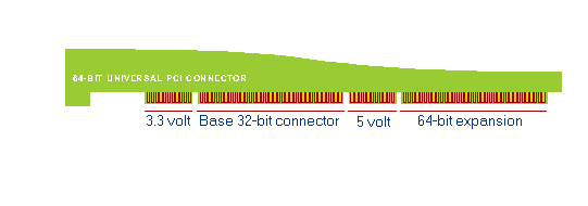
In addition, PCI systems may implement either the 32-bit or 64-bit connector. Most PCI buses implement only the 32-bit portion of the connector which consists of pins 1 through 62. Advanced systems which support 64-bit data transfers implement the full PCI bus connector which consists of pins 1 through 94.
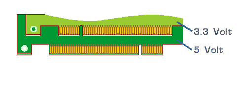
Low voltage evolution. The PCI specification also anticipates an eventual switchover from standard 5-volt logic to power-saving 3.3-volt operation. To accommodate the development of low voltage "green" PCs, PCI specifies two connector types and three different connector regimes a "5 Volt add-in boards" include a key notch in pin positions 50 and 51 to allow them to be plugged only into 5 Volt system connectors. "3.3 Volt add-in boards" include a key notch in pin positions 12 and 13 to allow them to be plugged only into 3.3 Volt system connectors. "Universal add-in boards" include both key notches to allow them to be plugged into either 5 Volt or 3.3 Volt system connectors. Universal boards must be able to adapt to operation at either signaling level.
A key on 5-volt sockets (blocking pins 50 and 51) prevents the insertion of 3.3-volt boards. (Five-volt boards have a slot corresponding to the key.) A key on 3.3-volt sockets (at pins 12 and 13) restricts the insertion to correspondingly slotted 3.3-volt boards. Boards capable of discriminating the two voltage regimes have slots in both places . Figure shows the arrangement of the edge connectors on PCI boards designed for different operating voltages.
32-bit PCI edge connector
The 64-bit implementation of PCI extends the edge connector to accommodate the additional required signals. The following figure shows this extended connector and the full implementation of all of its options.
Physical characteristics
PCI defines several variations on the basic expansion board. The specification defines two sizes of board, each with three connector arrangements (5-volt, 3.3-volt, and dual voltage). The two board sizes are based on traditional ISA expansion boards.
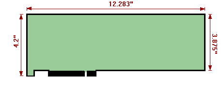
A full-size PCI expansion board measures 12.283 inches (312 mm) long. The main body of the board is about 3.875 inches high, although the expansion edge connector and a short skirt extend the width of the board to 4.2 inches (106.68 mm). The critical reference dimension is the centerline of the notch in the expansion connector, which is displaced 4.113 inches (104.47 mm) from the back edge (retaining bracket side) of the board. Figure 7.2 shows the dimensions of a full-size PCI board in 5-volt configuration. Cards designed for 3.3 volts or universal operation will differ in contact number and placement but not overall size.
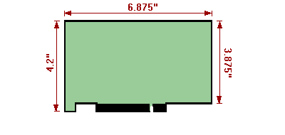
PCI also defines a short board, about half the length of a full-size board at 6.875 inches (174.63 mm) front to back. All other vital dimensions, including the distance from rear edge to the registration notch in the expansion connector are identical to a full-size board. Figure 7.3 show the dimensions of a PCI short card.
The following table illustrates the pinout definition for the PCI connector
|
Pin |
5V System Environment |
Pin |
3.3V System Environment |
Comments |
||||
|
Side B |
Side A |
Side B |
Side A |
|||||
|
1 |
-12V |
TRST# |
1 |
-12V |
TRST# |
32-bit start |
||
|
2 |
TCK |
+12V |
2 |
TCK |
+12V |
|||
|
3 |
Ground |
TMS |
3 |
Ground |
TMS |
|||
|
4 |
TDO |
TDI |
4 |
TDO |
TDI |
|||
|
5 |
+5V |
+5V |
5 |
+5V |
+5V |
|||
|
6 |
+5V |
INTA# |
6 |
+5V |
INTA# |
|||
|
7 |
INTB# |
INTC# |
7 |
INTB# |
INTC# |
|||
|
8 |
INTD# |
+5V |
8 |
INTD# |
+5V |
|||
|
9 |
PRSNT1# |
Reserved |
9 |
PRSNT1# |
Reserved |
|||
|
10 |
Reserved |
+5V (I/O) |
10 |
Reserved |
+3.3V (I/O) |
|||
|
11 |
PRSNT2# |
Reserved |
11 |
PRSNT2# |
Reserved |
|||
|
12 |
Ground |
Ground |
12 |
Connector Key |
3.3V key |
|||
|
13 |
Ground |
Ground |
13 |
Connector Key |
3.3V key |
|||
|
14 |
Reserved |
Reserved |
14 |
Reserved |
Reserved |
|||
|
15 |
Ground |
RST# |
15 |
Ground |
RST# |
|||
|
16 |
CLK |
+5V (I/O) |
16 |
CLK |
+3.3V (I/O) |
|||
|
17 |
Ground |
GNT# |
17 |
Ground |
GNT# |
|||
|
18 |
REQ# |
Ground |
18 |
REQ# |
Ground |
|||
|
19 |
+5V (I/O) |
Reserved |
19 |
+3.3V (I/O) |
Reserved |
|||
|
20 |
AD[31] |
AD[30] |
20 |
AD[31] |
AD[30] |
|||
|
21 |
AD[29] |
+3.3V |
21 |
AD[29] |
+3.3V |
|||
|
22 |
Ground |
AD[28] |
22 |
Ground |
AD[28] |
|||
|
23 |
AD[27] |
AD[26] |
23 |
AD[27] |
AD[26] |
|||
|
24 |
AD[25] |
Ground |
24 |
AD[25] |
Ground |
|||
|
25 |
+3.3V |
AD[24] |
25 |
+3.3V |
AD[24] |
|||
|
26 |
C/BE[3]# |
IDSEL |
26 |
C/BE[3]# |
IDSEL |
|||
|
27 |
AD[23] |
+3.3V |
27 |
AD[23] |
+3.3V |
|||
|
28 |
Ground |
AD[22] |
28 |
Ground |
AD[22] |
|||
|
29 |
AD[21] |
AD[20] |
29 |
AD[21] |
AD[20] |
|||
|
30 |
AD[19] |
Ground |
30 |
AD[19] |
Ground |
|||
|
31 |
+3.3V |
AD[18] |
31 |
+3.3V |
AD[18] |
|||
|
32 |
AD[17] |
AD[16] |
32 |
AD[17] |
AD[16] |
|||
|
33 |
C/BE[2]# |
+3.3V |
33 |
C/BE[2]# |
+3.3V |
|||
|
34 |
Ground |
FRAME# |
34 |
Ground |
FRAME# |
|||
|
35 |
IRDY# |
Ground |
35 |
IRDY# |
Ground |
|||
|
36 |
+3.3V |
TRDY# |
36 |
+3.3V |
TRDY# |
|||
|
37 |
DEVSEL# |
Ground |
37 |
DEVSEL# |
Ground |
|||
|
38 |
Ground |
STOP# |
38 |
Ground |
STOP# |
|||
|
39 |
LOCK# |
3.3V |
39 |
LOCK# |
3.3V |
|||
|
40 |
PERR# |
SDONE |
40 |
PERR# |
SDONE |
|||
|
41 |
+3.3V |
SBO# |
41 |
+3.3V |
SBO# |
|||
|
42 |
SERR# |
Ground |
42 |
SERR# |
Ground |
|||
|
43 |
+3.3V |
PAR |
43 |
+3.3V |
PAR |
|||
|
44 |
C/BE[1]# |
AD[15] |
44 |
C/BE[1]# |
AD[15] |
|||
|
45 |
AD[14] |
+3.3V |
45 |
AD[14] |
+3.3V |
|||
|
46 |
Ground |
AD[13] |
46 |
Ground |
AD[13] |
|||
|
47 |
AD[12] |
AD[11] |
47 |
AD[12] |
AD[11] |
|||
|
48 |
AD[10] |
Ground |
48 |
AD[10] |
Ground |
|||
|
49 |
Ground |
AD[09] |
49 |
M66EN |
AD[09] |
|||
|
50 |
Connector Key |
50 |
Ground |
Ground |
5V key |
|||
|
51 |
Connector Key |
51 |
Ground |
Ground |
5V key |
|||
|
52 |
AD[08] |
C/BE[0]# |
52 |
AD[08] |
C/BE[0]# |
|||
|
53 |
AD[07] |
+3.3V |
53 |
AD[07] |
+3.3V |
|||
|
54 |
+3.3V |
AD[06] |
54 |
+3.3V |
AD[06] |
|||
|
55 |
AD[05] |
AD[04] |
55 |
AD[05] |
AD[04] |
|||
|
56 |
AD[03] |
Ground |
56 |
AD[03] |
Ground |
|||
|
57 |
Ground |
AD[02] |
57 |
Ground |
AD[02] |
|||
|
58 |
AD[01] |
AD[00] |
58 |
AD[01] |
AD[00] |
|||
|
59 |
+5V (I/O) |
+5V (I/O) |
59 |
+3.3V (I/O) |
+3.3V (I/O) |
|||
|
60 |
ACK64# |
REQ64# |
60 |
ACK64# |
REQ64# |
|||
|
61 |
+5V |
+5V |
61 |
+5V |
+5V |
|||
|
62 |
+5V |
+5V |
62 |
+5V |
+5V |
32-bit end |
||
|
Connector Key |
Connector Key |
64-bit spacer |
||||||
|
Connector Key |
Connector Key |
64-bit spacer |
||||||
|
63 |
Reserved |
Ground |
63 |
Reserved |
Ground |
64-bit start |
||
|
64 |
Ground |
C/BE[7]# |
64 |
Ground |
C/BE[7]# |
|||
|
65 |
C/BE[6]# |
C/BE[5]# |
65 |
C/BE[6]# |
C/BE[5]# |
|||
|
66 |
C/BE[4]# |
+5V (I/O) |
66 |
C/BE[4]# |
+3.3V (I/O) |
|||
|
67 |
Ground |
PAR64 |
67 |
Ground |
PAR64 |
|||
|
68 |
AD[63] |
AD[62] |
68 |
AD[63] |
AD[62] |
|||
|
69 |
AD[61] |
Ground |
69 |
AD[61] |
Ground |
|||
|
70 |
+5V (I/O) |
AD[60] |
70 |
+3.3V (I/O) |
AD[60] |
|||
|
71 |
AD[59] |
AD[58] |
71 |
AD[59] |
AD[58] |
|||
|
72 |
AD[57] |
Ground |
72 |
AD[57] |
Ground |
|||
|
73 |
Ground |
AD[56] |
73 |
Ground |
AD[56] |
|||
|
74 |
AD[55] |
AD[54] |
74 |
AD[55] |
AD[54] |
|||
|
75 |
AD[53] |
+5V (I/O) |
75 |
AD[53] |
+3.3V (I/O) |
|||
|
76 |
Ground |
AD[52] |
76 |
Ground |
AD[52] |
|||
|
77 |
AD[51] |
AD[50] |
77 |
AD[51] |
AD[50] |
|||
|
78 |
AD[49] |
Ground |
78 |
AD[49] |
Ground |
|||
|
79 |
+5V (I/O) |
AD[48] |
79 |
+3.3V (I/O) |
AD[48] |
|||
|
80 |
AD[47] |
AD[46] |
80 |
AD[47] |
AD[46] |
|||
|
81 |
AD[45] |
Ground |
81 |
AD[45] |
Ground |
|||
|
82 |
Ground |
AD[44] |
82 |
Ground |
AD[44] |
|||
|
83 |
AD[43] |
AD[42] |
83 |
AD[43] |
AD[42] |
|||
|
84 |
AD[41] |
+5V (I/O) |
84 |
AD[41] |
+3.3V (I/O) |
|||
|
85 |
Ground |
AD[40] |
85 |
Ground |
AD[40] |
|||
|
86 |
AD[39] |
AD[38] |
86 |
AD[39] |
AD[38] |
|||
|
87 |
AD[37] |
Ground |
87 |
AD[37] |
Ground |
|||
|
88 |
+5V (I/O) |
AD[36] |
88 |
+3.3V (I/O) |
AD[36] |
|||
|
89 |
AD[35] |
AD[34] |
89 |
AD[35] |
AD[34] |
|||
|
90 |
AD[33] |
Ground |
90 |
AD[33] |
Ground |
|||
|
91 |
Ground |
AD[32] |
91 |
Ground |
AD[32] |
|||
|
92 |
Reserved |
Reserved |
92 |
Reserved |
Reserved |
|||
|
93 |
Reserved |
Ground |
93 |
Reserved |
Ground |
|||
|
94 |
Ground |
Reserved |
94 |
Ground |
Reserved |
64-bit end |
||